
LearnElectronics India
Top 5 PCB Designing Software.🙇♂️PCB design has grown in the field of electronics industry. 🧑🎓👩🏫
8 months ago - 0:57

OMICRON Lab
PCB Layout Fundamentals
4 years ago - 42:38

Robert Feranec
Do you also make these mistakes in PCB Layout?
2 months ago - 1:01:14

Maker's Fun Duck
ESP32-S3 PCB Design with KiCad: From Schematic to Manufacturing Step-by-Step
2 months ago - 15:05

Altium Academy
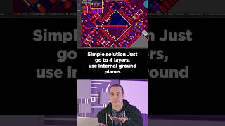
Types of PCB Grounding Explained | PCB Layout
2 years ago - 18:12

RayMing PCB
Why can't objects on the PCB be selected in KiCad?| PCB Design #23
2 days ago - 5:24

How To Mechatronics
EasyEDA - Free Electronics Circuit & PCB Design + Simulation Online Software Review
9 years ago - 4:38
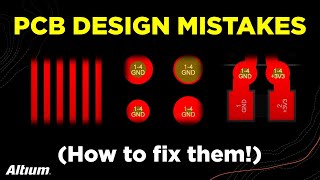
Altium Academy
Top 5 Beginner PCB Design Mistakes (and how to fix them)
2 years ago - 12:52

EEVblog
EEVblog #1323 - PCB Layout Review & Analysis
4 years ago - 37:29

Robert Feranec
Why is 50 OHM impedance used in PCB Layout? | Explained | Eric Bogatin | #HighlightsRF
3 years ago - 4:00

Robert Feranec
Ground in PCB Layout - Separate or Not Separate? (with Rick Hartley)
4 years ago - 1:03:20

LtlBiTech
Complete PCB Design Course in OrCAD and Allegro 17.4 | OrCAD & Allegro PCB Design by LtlBiTech
1 year ago - 9:02:56

The Hook Up
PCB Creation for Beginners - Start to finish tutorial in 10 minutes
3 years ago - 10:40

Robert Feranec
High Speed PCB Design Rules (Lesson 4 of Advanced PCB Layout Course)
10 years ago - 56:20

embed idea
5 best PCB design software you should try | Make great designs on your PCB | Embed Idea
4 years ago - 7:06
Project Crash
PCB Design #pcbdesign #electronics
2 years ago - 0:16

Robert Feranec
... PCB Layout, High Speed, Board Design and more ... Ask questions on our Discord: https://discord.gg/8a8dUcHmrx Sign up for ...
@RobertFeranec subscribers

Hans Rosenberg
Flawless PCB design: 3 simple rules - Part 2
11 months ago - 11:05

Robert Cox
Introduction to Basic Concepts in PCB Design
6 years ago - 25:54

Easy HomeMade Projects
EasyEDA - Free online Schematic & PCB Design Software + How to make a PCB
8 years ago - 9:37
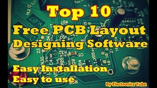
Electronics Tube
Best 10 Free PCB Layout design software for Easy PCB Designing latest 2018 by Electronics Tube
6 years ago - 2:22

Robert Feranec
How to improve your PCB Layout - Checking Nets
4 years ago - 52:32

NerdsElectro
EasyEDA Tutorial for Beginners | Component library #pcbdesign #electronicsdesign
8 months ago - 0:16

ECAREERPLUZ
PCB Design Training @ECAREERPLUZ
1 year ago - 0:31

Robert Feranec
Tutorial 3 for Altium Beginners: PCB Layout
6 years ago - 26:33
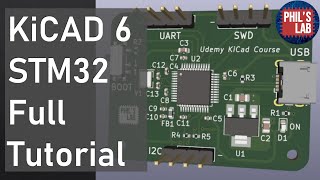
Phil’s Lab
KiCad 6 STM32 PCB Design Full Tutorial - Phil's Lab #65
3 years ago - 1:40:06

Robert Feranec
Review of a PCB Layout: Do you do same mistakes? - For Beginners (Part 1 of 4)
7 years ago - 15:11

PCB Power
What are the guidelines of analog PCB layout?
5 years ago - 0:26
Altium Academy
Gorgeous PCB Layout! | 1-Min #PCBDesign
1 year ago - 1:00

Altium Academy
Two Ways to Convert Gerber Files to a PCB Layout #pcbdesign #altium #altiumdesigner
2 years ago - 0:33

Phil’s Lab
How To Learn PCB Design (My Thoughts, Journey, and Resources) - Phil's Lab #87
2 years ago - 18:49
LtlBiTech
Complete PCB Design Course in OrCAD and Allegro 17.4 | OrCAD & Allegro PCB Design by LtlBiTech
1 year ago - 9:02:56

Hans Rosenberg
Flawless PCB design: RF rules of thumb - Part 1
11 months ago - 15:45

Robert Feranec
How To Improve Your PCB Layout - Power Planes
4 years ago - 43:41

Robert Feranec
Advanced PCB Layout - Online Course
10 years ago - 2:32

TryTronics
Pcb design for an inverter #pcb #electronics #altium #electronic#layout #tech#electrical#trytronics
2 years ago - 0:17

Biricha
PCB Layout Fundamentals
3 years ago - 42:38

My Embedded School
ESP32 pcb design easyeda #pcbdesign #myembeddedschool #easyeda #shorts
1 year ago - 0:16

solder butut
Unbelievably Simple PCB Design & Auto-Root Trick with Proteus!
2 years ago - 0:16

Autodesk Fusion
Mastering PCB Design with Quick Route Fanout | Autodesk Fusion 360
2 years ago - 0:13

DigiKey
Practical Guide High Speed PCB Layout
16 years ago - 0:46
Grease Pencil Blender
Free PRINTED CIRCUIT designer: SCHEMATIC, PCB LAYOUT, AUTOROUTE, GERBER
12 years ago - 0:43

Altium Academy
Vias-in-Pad Problems! | 1 Min PCB Design Review
2 days ago - 1:00

Phil’s Lab
2-Layer PCB Design Tips - Phil's Lab #137
1 year ago - 32:27

Jeremy Blum
Tutorial 2 for Eagle: Printed Circuit Board Layout
13 years ago - 31:48

Altium Academy
Two-Layer PCB Design Tips: Achieving the Optimal Layout
1 year ago - 21:32

Altium Academy
Altium Designer Quick-Start Tutorial with Phil Salmony from Phil's Lab
2 years ago - 23:37

DigiKey
Getting Started with PCB Layout #ShawnHymel #electronics #engineering #maker
1 year ago - 1:00

Life of Electronics
pcb layout design tutorial for beginners | Dual supply board - part 2
6 years ago - 13:32

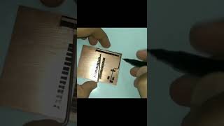
Aslam Hossain
PCB Toner Transfer from Tracing Paper using Heat | PCB Layout Design in Trace Paper #pcbdesign
6 months ago - 0:20

Hans Rosenberg
flawless PCB design: Bad ground ideas many engineers believe - Part 6
10 months ago - 15:11

Robert Feranec
Up to 255 Amps Power Supply Schematic and PCB Layout | Server Board Design | #HighlightsRF
3 years ago - 5:19

Altium Academy
PCB Layout Replication Demo: Streamline Your Design Process
1 year ago - 4:38

Narendra Jobs
Hiring High Speed PCB Layout Designer and Lead | Hardwar | VLSI
3 years ago - 0:11

Phil’s Lab
Aesthetic PCB Design Tips - Phil's Lab #84
2 years ago - 17:56
Altium Academy
Impressive Buck Converter Design! | 1 Min PCB Design Review
4 months ago - 1:27

PCB Power
PCB Layout to PCB Assembly, get your customized Printed Circuit Board ordered
4 years ago - 0:18
Altium Academy
EMI Filtering Needed! | 1 Min PCB Design Review
10 months ago - 0:58

PCB Power
PCB Layout to PCB assembly
4 years ago - 0:21

Doug Smith
Finding PCB layout defects
16 years ago - 3:03
Electronics hobbyy
PCB Design 🟢 | electronics hobbyy #engineer #electronics #electronics_hobbyy #maker #diy #pcb
3 years ago - 0:30

Hardware Unknown
How to Make a Circuit Board (Beginner's Guide)
3 years ago - 8:01

Easy HomeMade Projects
Learn PCB Designing Just in 15 Minutes! EasyEDA + JLCPCB Complete Tutorial 2023
2 years ago - 17:13

Dario Fresu
What is Impedance? - PCB Design and Signal Integrity
1 year ago - 9:26

Techpile
Hands-on PCB Design by Electronics Trainees Conducted by Techpile #techpile
8 months ago - 1:01

JLCPCB
Top tips for successful PCB Layout Desig #jlcpcb #shorts
1 year ago - 1:00

Nexlogic
PCB Design Layout Process Part 2
16 years ago - 2:59

TheTiaraTech Show
PCB Layout Design Part 1 | How to design PCB Layout | PCB Layout बनाने का तरीका | PCB Software
4 years ago - 10:17

Embedded System
PCB Layout designing using Eagle software
7 years ago - 9:50


