Robert Feranec
Tutorial OrCAD and Cadence Allegro PCB Editor | 2022 | Step by Step | For Beginners
3 years ago - 1:57:25

Robert Feranec
Starting with OrCAD and Cadence Allegro PCB - Tutorial for Beginners
8 years ago - 1:03:57

parsysEDA
OrCAD simple flow from schematic to PCB
7 years ago - 33:44

parsysEDA
OrCAD Simple PCB Design Tutorial 17.4
4 years ago - 47:39
Robert Feranec
Doing PCB Layout - Learn OrCAD & Cadence Allegro Essentials (Lesson 9)
6 years ago - 1:17:12

LtlBiTech
Complete PCB Design Course in OrCAD and Allegro 17.4 | OrCAD & Allegro PCB Design by LtlBiTech
1 year ago - 9:02:56

Circuit Analysis
Cadence OrCad PCB Editor 17.4 (Complete board layout in 30 min)
4 years ago - 29:55

FlowCADch
OrCAD/Allegro Quickplace
7 years ago - 1:08

LtlBiTech
How to create capacitor symbol in orcad | Learn PCB schematic #pcb #pcbdesign #orcad #course #udemy
1 year ago - 0:29

One Electron
OrCAD Capture Tutorial 05 Net Aliases
6 years ago - 1:45

FlowCAD
Why OrCAD
7 years ago - 3:03
Khurram Yousaf
OrCAD Basic PCB Design Tutorial Part 1 of 6
10 years ago - 9:31

Cadence Design Systems
How to create classes in the Constraint Manager using the OrCAD X Capture Schematic
11 months ago - 1:40

TechEdKirsch
How to Master the OrCAD PCB Editor Design Workflow + Free Cheat Sheet
4 years ago - 2:23

FlowCADch
OrCAD Symbol Editor
7 years ago - 1:34

LtlBiTech
How to draw resistor symbol in OrCAD? | PCB | PCB Design | Orcad PCB | IEEE symbol #pcb #electronics
11 months ago - 0:30

parsysEDA
OrCAD How-To - Picture Hierarchy Blocks Tutorial Cadence OrCAD Allegro
13 years ago - 1:13

FlowCADch
OrCAD/Allegro Place Replicate
7 years ago - 1:38

Shaer Ahmed
Tutorial 01 on OrCAD 9.2 - Introduction
9 years ago - 2:35

Electronics Engineering
How to create custom schematic symbols - OrCAD Capture CIS Tutorial (2019)
6 years ago - 2:34

LtlBiTech
Shortcut keys in OrCAD schematick | Learn Complete PCB Design #pcb #course #udemy #orcad #pcbdesign
1 year ago - 0:23
LtlBiTech
Complete PCB Design Course is now online | OrCAD/Allegro PCB Design Course #pcbdesign #pcb #course
1 year ago - 0:16
Electronics Engineering
How to set layers of PCB (Board Stack-up) - OrCAD PCB Editor Tutorial (2019)
6 years ago - 1:52

parsysEDA
Tutorial OrCAD Allegro Move Vias
8 years ago - 1:25
LtlBiTech
How to draw resistor symbol in OrCAD? | PCB | PCB Design | Orcad PCB | IEEE symbol #pcb #electronics
11 months ago - 0:30

Sunstream Global
OrCAD X Simulation for Accurate PCB Validation
4 months ago - 0:51

parsysEDA
OrCAD Capture Crossprobe Crossplace
5 years ago - 4:00

Creative ideas EEE
Symbols creative #orcad #circuits #circuits #design #labview #allegro
2 years ago - 0:30
LtlBiTech
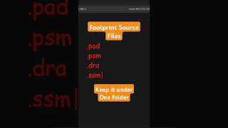
PCB Footprint Source Files in Allegro | Allegro PCB Design | Learn PCB Design #education #pcbdesign
7 months ago - 0:16
Chapter_B
Half Wave Rectifier #shorts #orcad #shortsfeed
1 year ago - 0:45

HaSofu Academy
Solving the Mysterious Problem with OrCAD Capture Design Templates - HaSofu Uncovers the Answer!
2 years ago - 2:17

One Electron
OrCAD Capture Tutorial 11 Generate a Smart PDF
6 years ago - 0:53

LtlBiTech
Calling Pins in Footprint | PCB Design Course | Footprints in Allegro #orcad #pcb #electrons #shorts
10 months ago - 0:19

C Roy
Orcad PCB Design Tutorial - 14 Create non standard PCB footprint
6 years ago - 4:00

GUI YUN
How to mass-replace schematic symbols in OrCAD Capture using Replace Cache and Update Cache?
3 months ago - 3:25

FlowCAD
Migration from Altium to OrCAD X - Translation of Schematics
11 months ago - 4:10

LtlBiTech
IEEE Standard Symbol Creation in OrCAD | 2-Pin Connector Symbol Creation #pcb #course #udemy #orcad
1 year ago - 0:30

GUI YUN
How to quickly extract schematic symbols from existing designs in OrCAD Capture?
3 months ago - 2:31

PCB Engineering
PCB Design Tutorial_55 Orcad Pcb Editor_Delete Unconnected Shapes
7 years ago - 1:47

Electronics Engineering
How to update existing footprints in board file- OrCAD PCB Editor Tutorial (2019)
6 years ago - 1:51

parsysEDA
OrCAD X Cloud enabled Circuit Design Component Management
1 year ago - 3:25

Nordcad
OrCAD/Allegro | Tech tip | 3D mapper in PCB Editor
2 years ago - 1:45

LtlBiTech
Solder mask creation in allegro PCB Design #orcad #allegro #pcbdesign #soldermask #footprints #pcb
11 months ago - 0:23

Punit Grewal
Orcad 16.5 Installation Method
12 years ago - 2:22
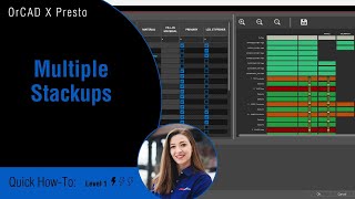
EMA Design Automation
Unleash the Power of Rigid-Flex PCB Designs in OrCAD X with MULTIPLE Stackups!
6 months ago - 4:04

ABC CAD Trainings
Master Orcad PSpice with ABC Trainings: Comprehensive Course for Beginners & Pros #orcad #pspice
1 year ago - 0:48

APSpace
How to import from SnapEDA to OrCAD Capture 17.4 and OrCAD PCB Editor: Tutorial 2
2 years ago - 6:28

C Roy
Orcad PCB Design Tutorial - 9 Create Artwork
6 years ago - 18:18
Wide Spectrum
Orcad Schematics - Create a new Library Part
6 years ago - 3:25

SarosPCB
PADS Schematic translation OrCAD, CADStar, Altium Designer, PCAD, Protel
13 years ago - 1:22
interCAD
OrCAD to PADS Cross Probing Selection
5 years ago - 3:24

Raan Dayzz
Orcad 16.6 Tutorial 3 | How to Design a simple schematic.
5 years ago - 4:51

Nam Hoàng
Orcad capture auto connect to bus, auto wire
8 years ago - 1:26

EMA Design Automation
Component Library Management in OrCAD X: How to Setup Your Designs for Success
8 months ago - 51:57

Q Learns
Bus in Orcad
5 years ago - 8:04

AlphaTech
OrCAD Capture CIS Video1 Create New Project & New Library
Introduction ...
7 years ago - 6:13

TechEdKirsch
OrCAD Tutorial - Create Gerber Artwork Files Faster Using Color View Saves
5 years ago - 3:06
HaSofu Academy
OrCAD X 24 PCB Editor How to Create Color Views and Files
9 months ago - 2:28

baios4
How to install Orcad 10.5 in Windows 7
10 years ago - 2:42

PCB Engineering
PCB Design Tutorial_57 Orcad Pcb Editor Fabrication Drawing Creation
7 years ago - 11:28

GUI YUN
How to export a custom BOM from OrCAD Capture?
3 months ago - 5:01

electroSome
Single Side PCB Designing using Orcad Layout 10.5
12 years ago - 5:57

C Roy
Orcad Tutorial | Design a custom footprint - part 1/2
4 years ago - 12:55

One Electron
OrCAD Capture Tutorial 01 New Project
6 years ago - 0:39

HaSofu Academy
How to add a 3D model to a PCB footprint in OrCAD X tactile switch
1 year ago - 3:22
Richard Binns
OrCAD schematic capture exmaple
16 years ago - 3:49

Ahsan Ali
Hardware PCB Design in OrCAD
4 months ago - 4:58